
Nuclear-Spin Flash Memory: Writing Data into the State of an Atomic Nucleus
From 3.3×10²⁹ bits of hot data per second to electron–nuclear spin transfer, the origin of the 100 ns write, parallel throughput, working temperature, residence time and four doping schemes
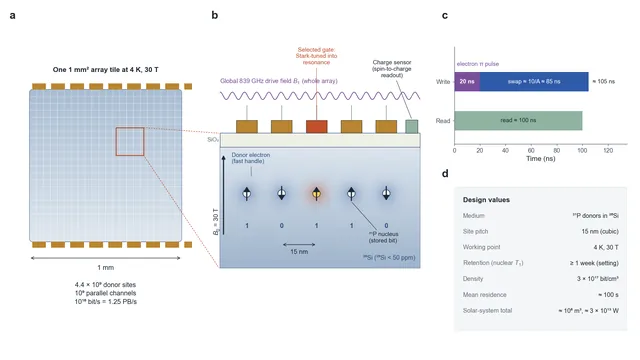
A nuclear-spin flash tile at 4 K and 30 T: gate-tuned phosphorus donors, a global drive field and a write of about 100 ns.
The carbon-isotope archive solves the problem of remembering. Each year about 10³⁵ bits of a civilisation's useful data are cast into diamond, written once and read forever. But that is only 1% of the total. In the year 2400 the Solar System produces about 3.3×10²⁹ bits of raw data every second: sensor streams, intermediate simulation results, drafts made by AI systems. These have to be written quickly, read several times and erased once they have been processed. For this data the storage has to hold information in a state of the atom, not in its structure.
There are many candidate states: electric charge, electron spin, nuclear spin. Charge leaks away. An electron spin forgets its orientation within milliseconds. The spin of an atomic nucleus inside a crystal can stay put for hours to days. Its one weakness is that it responds slowly: flipping it directly takes tens of microseconds. Pair the nucleus with a responsive electron and you get a memory that is both fast and retentive. This article works through such a memory for the world of The Digital Revolution: where its 100 ns write time comes from, how a billion sites can be driven in parallel, why it runs at 4 K in a 30 T field, how long data stays in it, and what it costs in energy and materials.
The reasoning uses three levels of support, and every key number below is labelled accordingly.
- Known physics (not negotiable): Zeeman energy, Rabi oscillation, hyperfine coupling, the Fourier bandwidth of a pulse, Boltzmann statistics, the Carnot limit on refrigeration and Landauer's principle.
- Experiment (adopted for the setting): single-shot readout of the electron and nuclear spin of a single phosphorus atom in silicon (Morello 2010; Pla 2012, 2013); electron-to-nuclear state transfer (Morton 2008); nuclear spin coherence of ionised donors in ²⁸Si lasting 39 minutes at room temperature (Saeedi 2013).
- Engineering extrapolation (setting): 10⁹ parallel channels, 100 ns readout, operation at 4 K in a 30 T background field, and about 10⁻¹⁹ J per operation. None of these is possible in the twenty-first century, but none violates physics.
The main findings
Writing one bit takes about 100 ns. An electron flip of about 20 ns plus an electron-to-nucleus transfer of about 85 ns. The transfer time is set by the hyperfine coupling constant A; the design rule used here is about 10/A, and for phosphorus A = 117.5 MHz.
1 ns is out of reach. A shorter pulse has a wider spectrum: at 1 ns it spans about 1 GHz and flips the neighbours too. Pulse energy scales as 1/τ and peak power as 1/τ². And the transfer step itself cannot be faster than about 10/A.
What is stored is the classical orientation of a nuclear spin, so retention depends on the longitudinal relaxation time T₁, not on the coherence time T₂. The setting takes at least one week, far longer than hot data needs.
The working point is 4 K and 30 T, with a magnet made from the metallic-hydrogen alloy of the setting. The electron Zeeman energy is then about 40 K, which makes readout reliable. At a practical 300 W of electricity per watt of cooling, all the flash memory in the Solar System draws about 3×10¹³ W, about 0.6% of the information budget.
A 1 mm² array delivers 1.25 PB/s. At 15 nm pitch it holds 4.4×10⁹ sites; 10⁹ parallel channels at 10⁷ operations per second give 10¹⁶ bit/s, about 17 times the node-local storage bandwidth of the Frontier supercomputer. An earlier concept for the film quoted 10 PB/s by confusing bits with bytes.
The density is about 3×10¹⁷ bit/cm³, only 1/34,000 of the carbon-isotope archive. Hot data can therefore stay for only about 100 seconds on average, and the whole Solar System needs about 10⁸ m³ of this memory.
Table 1. Design baseline
| Parameter | Value | Basis |
|---|---|---|
| Medium | ³¹P donors in isotopically purified ²⁸Si | Experiment |
| Site pitch | 15 nm (three-dimensional cubic lattice) | Setting |
| Working point | 4 K, 30 T background field | Setting (metallic-hydrogen alloy magnet, EP06) |
| Write | Electron π pulse about 20 ns + hyperfine transfer about 85 ns | Calculation / setting |
| Read | Spin-to-charge conversion with radio-frequency reflectometry, about 100 ns | Setting |
| Retention | At least 1 week (nuclear spin T₁) | Setting |
| Throughput of a 1 mm² array | 10¹⁶ bit/s (1.25 PB/s) | Calculation |
| Volume density | About 3×10¹⁷ bit/cm³ (about 1.7×10⁵ silicon atoms per bit) | Calculation |
| Mean residence of hot data | About 100 s | Setting |
1. 99% of the data needs somewhere fast and erasable
The data stream of 2400 has two layers: a raw stream of about 10³⁷ bits per year, and the roughly 1% of it that goes into the archive (see the estimate of the data explosion). As a rate, the raw stream is:
Most of this data lives for seconds to weeks. It is written, read a few times, compressed or distilled, and erased. The requirements on this layer of storage are the opposite of those on the archive:
Table 2. Requirements of hot storage and the archive
| Requirement | Carbon-isotope archive | Hot storage |
|---|---|---|
| Number of writes | Once | Unlimited |
| Write speed | Slow is acceptable | As fast as possible |
| Retention | A billion years | Seconds to weeks |
| Density | As high as possible | Enough is enough |
| Write authority | Single (Origin signature, setting) | Local and autonomous |
Today's NAND flash takes from tens of microseconds to milliseconds to program a page, and each cell survives only about 10³ to 10⁵ program–erase cycles. At a write rate of order 10²⁹ bits per second, any medium that wears out would be destroyed quickly. Hot storage needs a state that does not wear and that flips in nanoseconds.
2. The nucleus: stable, but sluggish
A spin in a magnetic field has two energy levels, separated by an energy that corresponds to a resonance frequency:
Table 3. The electron and the ³¹P nucleus compared
| Quantity | Electron | ³¹P nucleus | Ratio |
|---|---|---|---|
| Gyromagnetic ratio γ/2π | 27.97 GHz/T | 17.24 MHz/T | About 1,620 |
| Resonance frequency at 30 T | About 839 GHz | About 517 MHz | — |
| π pulse in a 1 mT drive field | About 36 ns | About 58 μs | About 1,620 |
| Coupling to the environment | Strong, easily disturbed | Weak, hardly disturbed | — |
The electron value is for the phosphorus donor in silicon (g = 1.9985). π-pulse times use the Rabi frequency of a linearly polarised drive field (Section 3).
The original concept said the electron's magnetic moment is 660 times that of the nucleus. That figure applies to the proton; for phosphorus-31 the ratio is about 1,620. Flipping the nuclear spin directly with radio waves takes tens of microseconds, not milliseconds. The reason the nucleus is slow is the same reason it is stable: it responds weakly to magnetic fields, so its surroundings also find it hard to disturb. The core idea of this memory is to accept that trade, and to operate the nucleus through a responsive handle.
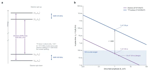
Figure 1. The phosphorus donor at 30 T. (a) Four spin levels, with the two electron-spin resonance lines near 839 GHz and the two nuclear lines near 458 and 576 MHz. (b) π-pulse time against drive-field amplitude for the electron and the nucleus.
3. The electron as a fast handle: where 100 ns comes from
A phosphorus atom has one more valence electron than silicon. That electron is loosely bound around the phosphorus nucleus, and the two are linked by the hyperfine coupling A. Writing happens in two steps.
Step one: flip the electron. In a drive field $B_{1}$ the electron's Rabi frequency and π-pulse time are:
With $B_{1}$ = 1.8 mT, $f_{R}$ ≈ 25 MHz and $t_{\pi}$ ≈ 20 ns.
Step two: hand the electron's state to the nucleus. This step runs through the hyperfine coupling, so its speed limit is set by A. One period of hyperfine precession is 1/A, about 8.5 ns for phosphorus, and a complete electron–nucleus swap built from hyperfine-conditioned operations takes several such periods. The design rule used here is about 10/A:
This rule is a setting assumption, not a measured law. In today's experiments the transfer uses separate nuclear radio-frequency pulses and takes microseconds or longer (Morton 2008); electrically driven electron–nuclear "flip-flop" transitions (Tosi 2017) point to faster routes. At 30 T the hyperfine interaction mixes the electron and nuclear states only weakly (A is about 10⁻⁴ of the electron Zeeman frequency), so the swap has to be driven actively.
Adding the two steps, 20 ns + 85 ns ≈ 100 ns is the time to write one bit. It is not a number tuned by fabrication; it follows from the density of the phosphorus electron's wavefunction at the nucleus. The original concept compared writing to pushing a millstone. The comparison can be made more precise: the push is slow not because the nucleus is heavy, but because the drive shaft between electron and nucleus, the hyperfine coupling, has only 117.5 MHz of strength.
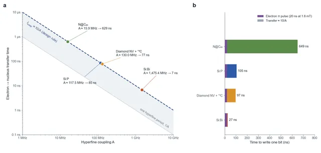
Figure 2. (a) Electron-to-nucleus transfer time against hyperfine coupling A. All four schemes lie on the same line, t ≈ 10/A: the larger A, the faster the write. The dotted line is one hyperfine period. (b) Total time to write one bit, electron flip plus transfer.
The same line explains the speed ranking of the four schemes in the original concept (Section 9). Bismuth's A is 12.5 times that of phosphorus, so it is fast. In N@C₆₀ the nitrogen atom sits at the centre of a carbon cage, the electron density at the nucleus is low and A is only 15.9 MHz, so it is slow.
4. Why not 1 ns
The first limit is frequency selectivity. The shorter the pulse, the wider its spectrum:
Table 4. Pulse length and spectral width
| Pulse | Spectral width | Consequence |
|---|---|---|
| 100 ns | About 10 MHz | Hits only the one site tuned into resonance |
| 10 ns | About 100 MHz | Starts to reach the resonance offsets of the neighbours |
| 1 ns | About 1 GHz | Flips a whole patch of neighbours: cross-talk |
The array uses local gates to tune a chosen phosphorus atom into resonance (next section), and the frequency offset the gates can produce is of order tens of MHz. The pulse bandwidth must be well below that offset; the 10 MHz of a 100 ns pulse leaves a margin. For a simple rectangular pulse, a neighbour detuned by 30 MHz is still flipped with a probability of up to about 3% (Figure 3a); shaped pulses and the read-back check in Table 9 deal with this residue.
The second limit is heat. For a fixed flip angle the drive field scales as $B_{1}\propto1/\tau$, the power as $B_{1}^{2}\propto1/\tau^{2}$, and the energy per pulse as $1/\tau$. Compressing 100 ns to 1 ns multiplies the energy per operation by 100 and the peak power by 10,000. At 4 K, every joule of heat costs about 300 J of electricity to remove (Section 6).
The third limit is the 10/A of Section 3: for phosphorus, the transfer step alone cannot be shorter than about 85 ns. So 100 ns is the speed at which three conditions hold together: no cross-talk, no overheating, complete transfer. Going faster means choosing an atom with a larger A.
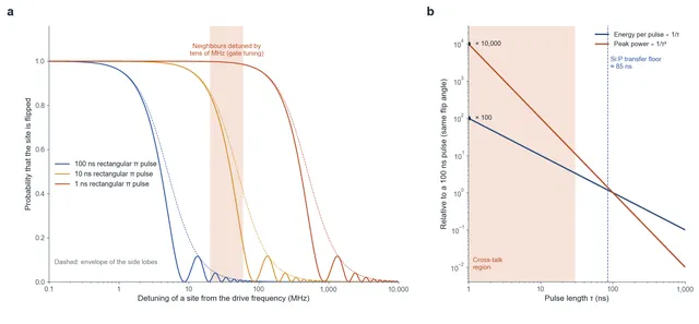
Figure 3. (a) Probability that a site is flipped by a rectangular π pulse, against its detuning from the drive, for pulses of 100, 10 and 1 ns. The shaded band marks neighbour detunings of tens of MHz. (b) Pulse energy and peak power relative to a 100 ns pulse.
5. Parallelism: one global field and a billion local gates
The original concept imagined nanowires firing microwaves at each atom. But at 839 GHz the wavelength is about 0.36 mm, and it cannot be focused onto 15 nm. The workable approach comes from Kane's 1998 proposal for a silicon quantum computer. A global field covering the whole array supplies the energy to flip spins, and a local gate above each site uses a voltage to shift that phosphorus atom's resonance frequency (the Stark effect), tuning it into or out of resonance. Only the sites tuned in are flipped; the others are left alone.
The concept's picture, in which fields overlap in space and reading and writing happen where the data is stored, still holds. The "billion microwave beams" simply become one field and a billion switches. The 15 nm pitch is set by the overlap of neighbouring donor electron wavefunctions: closer than that, the exchange coupling between neighbours makes sites interfere with each other.
Take 10⁹ parallel channels (leaving room for readout sensors and wiring), each completing one operation every 100 ns:
Table 5. Throughput compared
| System | Bandwidth | Ratio to a 1 mm² Si:P array |
|---|---|---|
| PCIe 5.0 NVMe SSD | About 14 GB/s | 1/89,000 |
| Enterprise all-flash array | About 100–200 GB/s | About 1/8,000 |
| Frontier node-local storage, total | About 75 TB/s | About 1/17 |
| Si:P array (1 mm²) | 1.25 PB/s | 1 |
The original concept's "10 PB/s, equal to 133 Frontiers" treated 10¹⁶ bits as 10¹⁶ bytes. Corrected, an array the size of a fingernail matches the storage bandwidth of about 17 Frontier systems, still the scale of an entire data centre today. Each gate's control line runs vertically down to a superconducting control layer beneath the array; the metallic-hydrogen alloy interconnects have zero resistance at 4 K and produce no Joule heating.
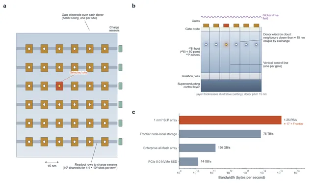
Figure 4. Array architecture. (a) Plan view: one gate electrode over each donor at 15 nm pitch, readout rows ending in charge sensors. (b) Cross-section: gates, gate oxide, ²⁸Si host with donors, vias and the superconducting control layer (thicknesses illustrative). (c) Bandwidth of a 1 mm² array compared with today's storage.
6. Readout and working temperature: why 4 K and 30 T
Readout uses spin-to-charge conversion. Only an electron with its spin up has enough energy to tunnel into a neighbouring charge sensor, and each tunnelling event is a measurable current pulse. This requires the electron's Zeeman energy to be much larger than the thermal energy:
Table 6. Background field and usable working temperature
| Background field | Zeeman energy (as a temperature) | Usable working temperature | Carnot work per joule removed, (300 − T)/T |
|---|---|---|---|
| 1.5 T (today's experiments) | 2.0 K | About 0.1–0.2 K | About 1,500–3,000 |
| 10 T | 13.4 K | About 1.3 K | About 230 |
| 30 T (setting) | 40.3 K | About 4 K | 74 |
Today's single-atom readout runs at about 0.1 K because laboratory magnets provide only 1–2 T. In the setting, the metastable metallic hydrogen alloy of EP06 has an upper critical field close to 200 T at 4 K, so a 30 T background magnet is well within its range. The working temperature can then rise to 4 K, and the minimum cooling work per joule falls by a factor of 20 to 40. The price is that the control frequency rises to about 839 GHz, in the terahertz band (the setting assumes precise terahertz pulses can be generated). The strong field is what moves nuclear-spin memory from the laboratory to the factory. Readout time is taken as about 100 ns, an extrapolation of radio-frequency reflectometry (setting).
Two side effects of the strong field are worth stating. The donor electron's own spin relaxation becomes much faster: the one-phonon process scales roughly as B⁵, and extrapolating from about a second at 1.5–2.5 T gives a few microseconds at 30 T. That is still well above the 100 ns operations, and it is one more reason the electron serves only as a short-lived handle while the nucleus holds the data. And the field squeezes the donor wavefunction somewhat (the magnetic length at 30 T is about 4.7 nm, against a donor radius of about 2 nm), which shifts A and the gate tuning by an amount this estimate does not compute.
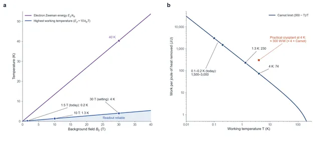
Figure 5. The working point. (a) Electron Zeeman energy and the highest working temperature for reliable readout (Zeeman energy ten times the thermal energy) against background field. (b) Minimum work to remove one joule of heat at temperature T and reject it at 300 K, with a practical 4 K cryoplant for comparison.
7. Retention: look at T₁, not T₂
Quantum computing cares about the coherence time T₂, how long the phase of a superposition survives. Storing a classical bit only requires the nuclear spin to stay up or down, and that is governed by the longitudinal relaxation time T₁. T₂ can never exceed 2T₁, and for nuclear spins in a quiet crystal T₁ is usually far longer than T₂. Experimentally, the nuclear spins of ionised phosphorus donors in isotopically purified ²⁸Si keep their coherence for 39 minutes even at room temperature, and for about 3 hours at cryogenic temperature (Saeedi 2013).
The setting takes a retention time of at least one week, on two conditions. First, the ²⁹Si in the silicon host (4.7% in natural silicon, and carrying a nuclear spin) must be reduced below 50 ppm, so that the host is magnetically quiet. Second, between reads and writes the donor electron is kept ionised, so that it does not disturb the nucleus. This is the same logic as the purified ¹²C of the carbon archive: both kinds of storage need a host with no nuclear spins. A week is far longer than hot data stays, so the memory never needs to be refreshed continuously the way DRAM does.
8. Capacity: why hot data can stay only about 100 seconds
The volume density of a 15 nm cubic lattice is:
That is about 1.7×10⁵ silicon atoms per bit, and 1/34,000 of the density of the carbon-isotope archive (10²² bit/cm³). The amount of hot data to be held equals the production rate times the residence time:
Table 7. Residence time and the total volume of flash in the Solar System (2400)
| Mean residence | Bits to hold | Flash volume | Equivalent cube |
|---|---|---|---|
| 1 s | 3.3×10²⁹ | 1.1×10⁶ m³ | 103 m on a side |
| 100 s | 3.3×10³¹ | 1.1×10⁸ m³ | About 480 m on a side |
| 1 h | 1.2×10³³ | 4.0×10⁹ m³ | About 1.6 km on a side |
| 1 day | 2.8×10³⁴ | 9.5×10¹⁰ m³ | About 4.6 km on a side |
The longer data stays in hot storage, the more silicon it needs. The setting takes a mean residence of about 100 seconds. In that time the raw stream is compressed, distilled and filtered; the useful 1% goes to a local casting module, authorised by Origin, that writes it into archive blocks, and the rest is erased. All the nuclear-spin flash in the Solar System then comes to about 10⁸ m³, spread across the data centres. Storage that moves trades density for speed, storage that stays trades speed for density, and the two divide the work by residence time.
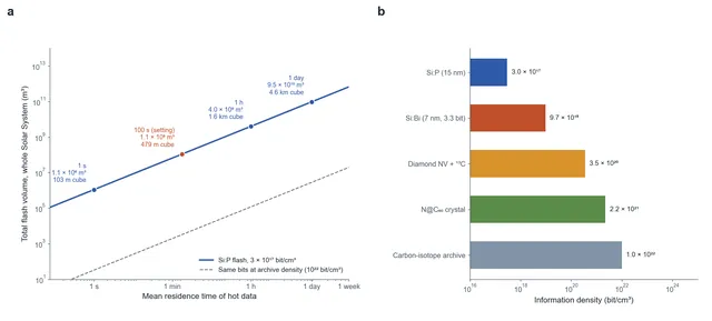
Figure 6. (a) Total flash volume needed in the Solar System against the mean residence time of hot data, for Si:P at 3×10¹⁷ bit/cm³ and, for comparison, at the archive density. (b) Information density of the four schemes and of the carbon-isotope archive.
9. Four schemes: trade-offs under one rule
Table 8. Four electron–nuclear spin schemes (checked)
| Scheme | Hyperfine A | Transfer ≈ 10/A | Write one bit | Bits per nucleus | Atoms per bit | Notes |
|---|---|---|---|---|---|---|
| Si:P (basic) | 117.5 MHz | About 85 ns | About 100 ns | 1 | About 1.7×10⁵ (15 nm) | Most mature; baseline of this article |
| Si:Bi (advanced) | 1,475 MHz | About 7 ns | About 30 ns | 3.3 (I = 9/2, 10 levels) | About 5,000 (about 7 nm) | Bismuth donor binds more tightly, can be packed closer |
| Diamond NV (high precision) | Nearest ¹³C about 130 MHz | About 77 ns | About 100 ns | About 10 ¹³C per NV | About 500 | Can work at high temperature; optical readout about 1 μs or more |
| N@C₆₀ (ultimate) | 15.9 MHz | About 630 ns | About 650 ns | 1.6 (¹⁴N, I = 1) | About 40–60 | Densest by molecular self-assembly; single-molecule readout hardest |
Write time = electron π pulse (about 20 ns) + transfer. Atoms per bit for N@C₆₀: 61 atoms per molecule divided by 1.6 bits gives about 40 with every molecule filled.
After checking, both the speed ranking and the density ranking of the original concept hold, with four corrections. NV centres in diamond are read by counting fluorescence photons, which takes at least about 1 μs per attempt (single-shot readout of a nuclear spin needs many repetitions), not 10 ns. The bismuth "twentyfold jump in density" comes from two factors multiplied together: each nucleus stores 3.3 bits, and the tighter binding allows a pitch of about 7 nm; together they give about 30 times the density of Si:P. Writing a bit into Si:Bi takes about 27 ns, not 20, once the electron flip is included. And an N@C₆₀ write cannot be shorter than its own 630 ns transfer; with the flip it is about 650 ns.
The industrial workhorse of 2400 is Si:P: it is the most mature on silicon processes and has the most reliable readout. Si:Bi serves computing caches that need faster writes, and N@C₆₀ is reserved for uses where density comes first.
10. Energy: after cooling, the cost of erasure returns to room temperature
The energy deposited at 4 K per operation is set at about 10⁻¹⁹ J (in a superconducting resonator most of the drive energy can be recovered). At a practical 300 W/W of refrigeration (about four times the Carnot value of 74):
The factor of 3 counts three operations per bit: write, read and verify. The total is about 0.6% of the 2400 information-industry budget of 4.8×10¹⁵ W.
Erasure also has a thermodynamic floor. Resetting a nuclear spin to a known state erases one bit. At 4 K this releases only $k_{B}$(4 K) ln 2 of heat, but the minimum work to carry that heat back up to room temperature brings the total to exactly $k_{B}$(300 K) ln 2. Cooling cannot get around Landauer's principle; this is the problem taken up in the article on reversible computing. For the whole raw stream that floor is about 10⁹ W, so the 3×10¹³ W of the flash memory sits about four orders of magnitude above it.
11. Materials: not a consumable
Nuclear-spin flash can be rewritten without limit, so the material is a one-time investment. The 1.1×10⁸ m³ of flash needs about 2.6×10⁸ t of silicon and about 1,700 t of phosphorus. The asteroid belt (about 2–3×10²¹ kg in total) holds a few times 10²⁰ kg of silicon, about 10⁴⁶ atoms, and of order 10¹⁸ kg of phosphorus, both far more than needed (see mining the asteroid belt). The real threshold is isotope purification: ²⁸Si must be enriched above 99.995%, removing the ²⁹Si. This shares an isotope-separation industry with the ¹²C purification of the carbon archive.
12. Main failure modes
Table 9. Failures and responses
| Failure | Trigger | Consequence | Design response |
|---|---|---|---|
| Loss of temperature control | Refrigeration fault; temperature rises above 10 K | Readout fidelity drops; misreads | Hot data stays only briefly; degrade to read-only and migrate out |
| Background magnet quench | Magnet fault | Zeeman splitting vanishes; reading and writing stop | Large margin of the metallic-hydrogen alloy magnet at 4 K; independent magnets per zone |
| Cross-talk | Pulse too short or gate tuning too weak | Neighbouring sites flipped by mistake | Pulses of at least 100 ns; read back and verify after each write |
| Nuclear spin relaxation | Residual ²⁹Si; stray electrons | Shorter retention | ²⁹Si below 50 ppm; donor electrons kept ionised |
| Ionising radiation | Cosmic rays create free charge | Local bit errors | Shielding; error-correcting codes; short residence limits error build-up |
| Control-layer fault | Damaged gate or readout line | Channel lost | Sites outnumber channels about 4.4 to 1; spare sites and channels are remapped |
13. Closing
The carbon archive and nuclear-spin flash are two sides of one coin. One writes information into the identity of an atom, the other into the orientation of a nucleus. One stays unchanged for a billion years, the other flips ten million times a second. Both depend on placing atoms precisely and on a magnetically quiet isotopic host, and both push storage to within a few orders of magnitude of the single atom. That settles the question of storage. The next question is what kind of machine computes on 3×10²⁹ bits a second; the optical computing GPU takes it up.
References and calculation basis
- B. E. Kane (1998), A silicon-based nuclear spin quantum computer, Nature 393: addressing by a global field and local gates (Stark tuning).
- A. Morello et al. (2010), Single-shot readout of an electron spin in silicon, Nature 467: spin-to-charge conversion readout.
- J. J. Pla et al. (2012), A single-atom electron spin qubit in silicon, Nature 489.
- J. J. Pla et al. (2013), High-fidelity readout and control of a nuclear spin qubit in silicon, Nature 496.
- J. J. L. Morton et al. (2008), Solid-state quantum memory using the ³¹P nuclear spin, Nature 455: electron–nuclear state transfer.
- K. Saeedi et al. (2013), Room-temperature quantum bit storage exceeding 39 minutes using ionized donors in silicon-28, Science 342.
- G. W. Morley et al. (2010), The initialization and manipulation of quantum information stored in silicon by bismuth dopants, Nature Materials 9: Bi donor A ≈ 1,475 MHz, I = 9/2.
- G. Tosi et al. (2017), Silicon quantum processor with robust long-distance qubit couplings, Nature Communications 8: electrically driven electron–nuclear flip-flop transitions.
- M. Fuechsle et al. (2012), A single-atom transistor, Nature Nanotechnology 7: deterministic placement of single phosphorus atoms.
- Oak Ridge Leadership Computing Facility, Frontier: aggregate node-local NVMe read bandwidth of about 75 TB/s.
- Calculation basis: γₑ/2π = 27.97 GHz/T (Si:P donor, g = 1.9985), γ(³¹P)/2π = 17.24 MHz/T; A(³¹P) = 117.53 MHz, A(N@C₆₀) ≈ 15.9 MHz; silicon 4.99×10²² atoms/cm³ and 2,329 kg/m³; Boltzmann and Planck constants from CODATA 2018. The transfer time of about 10/A is a design rule (setting). The 2400 raw stream of 3.3×10²⁹ bit/s and the 4.8×10¹⁵ W information budget come from the EP07 setting baseline; 10⁻¹⁹ J per operation, 300 W/W practical refrigeration and 100 s residence are setting values.
Appendix A. Principal symbols
Table 10. Symbols
| Symbol | Meaning | Symbol | Meaning |
|---|---|---|---|
| γ, $\gamma_{e}$ | Gyromagnetic ratio; electron gyromagnetic ratio | A | Hyperfine coupling constant |
| B, $B_{1}$ | Background field; drive field | $t_{\pi}$ | π-pulse time |
| $f_{R}$ | Rabi frequency | $t_{swap}$ | Electron–nucleus swap time |
| τ, Δf | Pulse length; spectral width | $E_{Z}$ | Electron Zeeman energy |
| T₁, T₂ | Longitudinal relaxation time; coherence time | Φ | Array throughput |
| ρ | Volume information density | $R_{raw}$ | Raw data production rate |